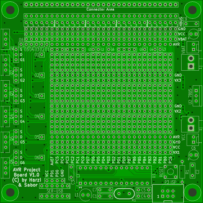
This is a PCB for prototyping with an ATmega*8 microcontroller. Eg. build a stable prototype of an AVR project, that have been created on a bread board or Arduino before.
| Name | Value | Description |
| C2 | 100nF | Blocking capacitor for AVR. |
| C3 | 100nF | AREF capacitor. |
| C6 | >= 10uF | VCC capacitor. |
| C7 | 100nF | VCC capacitor. |
| C8 | >= 10uF | VBAT capacitor (add only when VBAT is needed). |
| C9 | 100nF | VBAT capacitor (add only when VBAT is needed). |
| P3 | 2x3pin | Programming connector. |
| R1 | 10k | Pull-up resistor for reset. |
| SW1 | 6*6mm | Reset button. |
| U1 | ATmega*8 | Microcontroller. |
| Optional Crystal | ||
| X1 | 18.432MHz | or your preferred frequency. |
| C4, C5 | 22pF | Capacitors for the crystal. |
| AVCC Filter (Jumper J1 needs to become opened) | ||
| L1 | ??? | Filtering inductor. |
| C1 | 100nF | Blocking capacitor. |
| Varia | ||
| Q1-6 | IRL3705 / IRF4905 | Power transistors/MOSFET's. |
| U2 | 7805 (LM1117 or similar regulator) | +5V voltage regulator (don't forget to add C8 & C9). |
| small power connector | 1=GND, 2=V+. KF2510 (also to be used for connector area on the top). | |
| large power connector | 1=GND, 2=V+. VH 3.96mm (when there is more equipment using Vbat, the small connector should be used to distribute power to it). | |
| Name | Signal | Description |
| J1 | AVCC | Disconnects VCC from AVCC to add appropriate induction L1. Also add C1 = 100nF |
| J2 | VX2 | Connects VCC or VBAT to the VX2 line on the project area. |
| J3 | VX3 | Connects VCC or VBAT to the VX3 line on the project area. |
| J4 | PB6 | Connects PB6 (crystal) to the AVR lines on the project area. |
| J5 | PB7 | Connects PB7 (crystal) to the AVR lines on the project area. |
| J6 | PC6 | Connects /RESET to the AVR lines on the project area. |
| J7 | J7V | Connects VCC or VBAT to J7V of J9, J11, J13. |
| J8 | J8V | Connects VCC or VBAT to J8V of J10, J12, J14. |
| J9 | Q1S | Connects GND or J7V to the source of Q1. |
| J10 | Q2S | Connects GND or J8V to the source of Q2. |
| J11 | Q3S | Connects GND or J7V to the source of Q3. |
| J12 | Q4S | Connects GND or J8V to the source of Q4. |
| J13 | Q5S | Connects GND or J7V to the source of Q5. |
| J14 | Q6S | Connects GND or J8V to the source of Q6. |
| J15 | VX1 | Connects VBAT to the VX1 line on the project area. |
| J16 | AREF | Connects AREF to the AVR lines on the project area. |
The HBUS can be used to horizontally distribute signals nearby the connector area. All "1" are connected to each other, all "2" and so on. 5 times up to 6 signals may be distributed.
If you are using that monstrosity called Arduino the following table might come in handy for translating those ridiculous pin names. Please also make sure you use Arduino compatible resistors, LEDs, etc.
| DIL Pin | AVR Port | Functions | Arduino |
| 2 | PD0 | RXD | digital pin 0 |
| 3 | PD1 | TXD | digital pin 1 |
| 4 | PD2 | INT0 | digital pin 2 |
| 5 | PD3 | OC2B, INT1 | digital pin 3 |
| 6 | PD4 | XCK, T0 | digital pin 4 |
| 11 | PD5 | OC0B, T1 | digital pin 5 |
| 12 | PD6 | OC0A, AIN0 | digital pin 6 |
| 13 | PD7 | AIN1 | digital pin 7 |
| 14 | PB0 | CLKO, ICP1 | digital pin 8 |
| 15 | PB1 | OC1A | digital pin 9 |
| 16 | PB2 | SS, OC1B | digital pin 10 |
| 17 | PB3 | MOSI, OC2A | digital pin 11 |
| 18 | PB4 | MISO | digital pin 12 |
| 19 | PB5 | SCK | digital pin 13 |
| 23 | PC0 | ADC0 | analog input 0 |
| 24 | PC1 | ADC1 | analog input 1 |
| 25 | PC2 | ADC2 | analog input 2 |
| 26 | PC3 | ADC3 | analog input 3 |
| 27 | PC4 | ADC4, SDA | analog input 4 |
| 28 | PC5 | ADC5, SCL | analog input 5 |