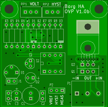
The Overvoltage PCB protects sensitive circuits from malfunctioning step down converters or other power supplies producing a too high voltage.
| Name | Value | Description |
| C1 | 100uF | Block capacitor. |
| C2 | 100n | Block capacitor. |
| D2 | LED | Lights up when the switch is on. |
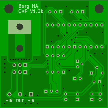
| P1 | CONN_3 | -In, Output, +In. |
| P2 | TESTPOINT | Measurement, Hysteresis, reference voltages. |
| R2 | 10k | Upper resistor of divider for reference voltage. |
| R4 | 56k | Hysteresis feedback resistor. |
| R5 | 120k | Measurement feedback resistor. |
| R6 | 1k | Current limiter for LED. |
| R9 | 18k | Lower resistor for divider of input voltage. |
| RP1 | 100k | Potentiometer in divider of input voltage. |
| RP2 | 100k | Potentiometer in hysteresis feedback. |
| U2 | TL072 | OPAMP. |
| Positive Rail Switched | ||
| D1 | 12V | Limits gate voltage, only needed if input voltage > 12VDC. |
| Q1 | IRF4905 | Power transistor for switching positiv rail. |
| Q3 | 2N3904 | Inverter and driver for power transistor. |
| R1 | 10k | Pullup for the gate of the power transistor. |
| R7 | 1.2k | Current limiting resistor for the gate driver. |
| Negative Rail Switched | ||
| Q2 | IRL3705 | Power transistor for switching the negative rail. |
| Input Voltage < 15VDC | ||
| D3 | 5.6V | Zener diode for the reference voltage. |
| J1 | LOWVOLT | Powers the circuit directly if set. |
| R3 | 0R | Upper resistor for the divider of the input voltage. |
| Input Voltage > 15VDC | ||
| C3 | 10uF | Block capacitor. |
| C4 | 100n | Block capacitor. |
| R3 | 15k | Upper resistor for the divider of the input voltage. |
| R8 | 10k | Lower resistor of divider for reference voltage. |
| U1 | 78L12 | Voltage regulator. |
Components are ordered by placement on the PCB, from top to bottom, from left to right.
| Voltage: | Vin < 15V | Vin > 15V | ||
| Switched Rail: | - | + | - | + |
| RP1 | 100k | |||
| RP2 | 100k | |||
| R3 | 0Ω | 15k | ||
| R5 | 120k | |||
| R4 | 56k | |||
| R6 | 1k | |||
| R1 | - | 10k | - | 10k |
| D1 | - | 12V | - | 12V |
| R2 | 10k | |||
| R7 | - | 1.2k | - | 1.2k |
| R9 | 18k | |||
| R8 | - | 10k | ||
| D3 | 5.6V | - | ||
| Q3 | - | 2N3904 | - | 2N3904 |
| U2 | TL072 | |||
| Q1 | - | IRF4905 | - | IRF4905 |
| Q2 | IRL3705 | - | IRL3705 | - |
| U1 | - | 78L12 | ||
| J1 | CLOSED | - | ||
| D2 | LED | |||
| C4 | - | 100n | ||
| C3 | - | 10uF | ||
| C1 | 100uF | |||
| C2 | 100n | |||
| P2 | MEAS, HYST, VREF | |||
| P1 | -In, Out, +In | |||