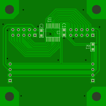

This level translator PCB is used to translate between two digital logic voltage levels, for example between 3.3V and 5V.


Schema, production files in the format needed for Seeed Studio.
The device with the lower voltage has to be connected to port A, the device with the higher voltage to port B. The translation is bidirectional, it automatically detects which side is drivin the line. The translator can be switched to tri-state by pulling OE low.
| 1 | GND | Power ground. |
| 2 | VCCA | Power supply for port A, 1.2V - 3.6V. |
| 3 | A1 | Port A pin 1. |
| 4 | A2 | Port A pin 2. |
| 5 | A3 | Port A pin 3. |
| 6 | A4 | Port A pin 4. |
| 7 | A5 | Port A pin 5. |
| 8 | A6 | Port A pin 6. |
| 9 | A7 | Port A pin 7. |
| 10 | A8 | Port A pin 8. |
| 1 | GND | Power ground. |
| 2 | VCCB | Power supply for port B, 1.65V - 5.5V. |
| 3 | B1 | Port B pin 1. |
| 4 | B2 | Port B pin 2. |
| 5 | B3 | Port B pin 3. |
| 6 | B4 | Port B pin 4. |
| 7 | B5 | Port B pin 5. |
| 8 | B6 | Port B pin 6. |
| 9 | B7 | Port B pin 7. |
| 10 | B8 | Port B pin 8. |
| 1 | GND | Power ground. |
| 2 | VCCA | Power supply for port A, 1.2V - 3.6V. |
| 3 | VCCB | Power supply for port B, 1.65V - 5.5V. |
| 4 | OE | Output enable, pulled high by a 10k resisstor. |
| 1 | GND | Power ground. |
| 2 | VCCA | Power supply for port A, 1.2V - 3.6V. |
| 3 | VCCB | Power supply for port B, 1.65V - 5.5V. |
| 4 | OE | Output enable, pulled high by a 10k resisstor. |
| Ref. | Count | Description |
|---|---|---|
| - | 1 | Borg Level Translator PCB |
| U1 | 1 | TXB0108 |
| C1, C2 | 2 | 100nF block capacitor, 0805. |
| R1 | 1 | 10k resistor, 0805. |
| P1, P2 | 2 | 10 pin IDC connector or pin headers. |
| P3, P4 | 2 | 4 pin 2510 connector or pin headers. |