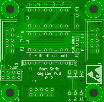
This shift register PCB can be assembled in two ways, either with a 74165 to get 8 inputs or with a 74595 to get 8 outputs. It can be connected to an SPI bus using additional lines for loading and storing the data. Multiple boards can be cascaded. The limit is only the driving capability of the clock, load and store output.
Schema, production files in the format needed for Seeed Studio.
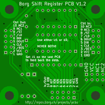
The boards can be connected to a chain, input and output boards can be mixed. Connect the controller to P1 of the first board. Then Connect P2 to P1 of the next board using a 1:1 cable, and so on. On the last board set the jumper J1 to feed back the data from the last PCB to the controller. The inputs/outputs are on P3 and P4.
All data is always shifted through all registers no matter if they are inputs or outputs. So if the chain consists of an input shift register followed by an output shift register alwyas 16 bits have to be shifted through. The first bit sent ends up in output 8, the 8th bit in output 1, the following 8 bit will be stored in the input register and have no effect. The first 8 bit read from the register come from the output register and can be ignored. The next 8 bit contain the inputs, input 8 first and input 1 last.
To use the shift register PCB with SPI make the following connections:
| Controller | Shift Register PCB |
| GND | GND |
| VCC | VCC |
| GPIO 1 | /MR |
| SCK | SHCP |
| MOSI | DIN |
| MISO | DOUT |
| GPIO 2 | /PL |
| GPIO 3 | STCP |
| - | NC1 |
| - | NC2 |
| 1 | GND | Power ground. |
| 2 | VCC | Power supply. HC: 2.0V - 5.5V. HCT: 4.5V - 5.5V. |
| 3 | /MR | Master reset of 74595, low active. |
| 4 | SHCP | Shift the register on the rising edge. |
| 5 | DIN | Serial data input to the shift register. |
| 6 | DOUT | Serial data out. |
| 7 | /PL | Load inputs into shift register, low active. |
| 8 | STCP | Store shift register in output registers on the rising edge. |
| 9 | NC1 | Not connected, just fed through to P2 and P4. |
| 10 | NC2 | Not connected, just fed through to P2 and P4. |
| 1 | GND | Power ground. |
| 2 | VCC | Power supply output. |
| 3 | /MR | Fed through from P1. |
| 4 | SHCP | Fed through from P1. |
| 5 | DOUT | Serial data out from the shift register. |
| 6 | DIN | Fed through to DOUT on P1. |
| 7 | /PL | Fed through from P1. |
| 8 | STCP | Fed through from P1. |
| 9 | NC1 | Fed through from P1. |
| 10 | NC2 | Fed through from P1. |
| 1 | GND | Power ground. |
| 2 | VCC | Power supply output. |
| 3 | 1 | Input/output 1. |
| 4 | 2 | Input/output 2. |
| 5 | 3 | Input/output 3. |
| 6 | 4 | Input/output 4. |
| 7 | 5 | Input/output 5. |
| 8 | 6 | Input/output 6. |
| 9 | 7 | Input/output 7. |
| 10 | 8 | Input/output 8. |
Some extra power pins and the "not connected" pins for free use.
| 1 | GND | Power ground. |
| 2 | GND | Power ground. |
| 3 | VCC | Power supply output. |
| 4 | VCC | Power supply output. |
| 5 | NC1 | Not connected 1. |
| 6 | NC1 | Not connected 1. |
| 7 | NC2 | Not connected 2. |
| 8 | NC2 | Not connected 2. |
Jumper J1 connects DOUT on P2 with DIN on P2. It has to be set on the last board in the chain to feed back the serial data to the controller. On all other boards it must not be set. In Position 1-2 it feeds back the output voltage of Q7 directly. In Position 2-3 it feeds back the output voltage of Q7 reduced by the level translator D1/D2/R1.
D1, D2, and R1 are optional, they are only needed if a level translator for the DOUT feedback pin is needed, and only on the last PCB in the chain.
| Ref. | Count | Description |
|---|---|---|
| - | 1 | Borg Shift register PCB |
| U1 | 1 | 74HC595 |
| U2, U3 | 0 | not used |
| P1, P2, P3 | 3 | 10 pin IDC connectors. |
| P4 | 1 | 10 pin screw terminal, 5mm spacing. |
| J1 | 1 | Jumper |
| C1 | 1 | 100nF block capacitor. |
| D1 | 1 | 3.3V Z-diode (optional) |
| D2 | 1 | BAT43 or 1N4148 (optional) |
| R1 | 1 | 1k resistor (optional) |
| Ref. | Count | Description |
|---|---|---|
| - | 1 | Borg Shift register PCB |
| U1 | 0 | not used |
| U2 | 1 | 74HC165 |
| U3 | 1 | 10k resistor network, 8 resistors with common pin. |
| P1, P2, P3 | 3 | 10 pin IDC connectors. |
| P4 | 1 | 10 pin screw terminal, 5mm spacing. |
| J1 | 1 | Jumper |
| C1 | 1 | 100nF block capacitor. |
| D1 | 1 | 3.3V Z-diode (optional) |
| D2 | 1 | BAT43 or 1N4148 (optional) |
| R1 | 1 | 1k resistor (optional) |
Note: Standard configuration of U3 is as pull up resistors. It can be mounted as pull down, then the common pin goes into the GND pad next to U3.